ALD: The Technique
|
Thin Film Deposition: Thin Film Deposition refers to the application of very thin films of material (e.g. a metal, or a metal oxide or nitride etc.) onto the surface of a substrate (e.g. a silicon wafer), and is an essential technique for technological device fabrication (e.g. fabrication of computer microprocessors, memory devices, optical communications components, etc.). Thin film deposition can be achieved using various techniques, including ALD, PVD and CVD (see below).
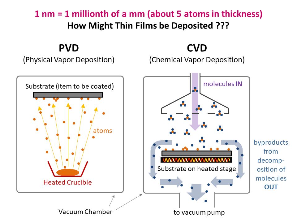
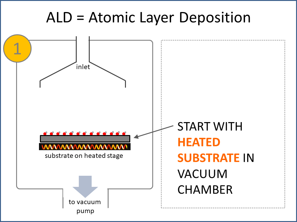
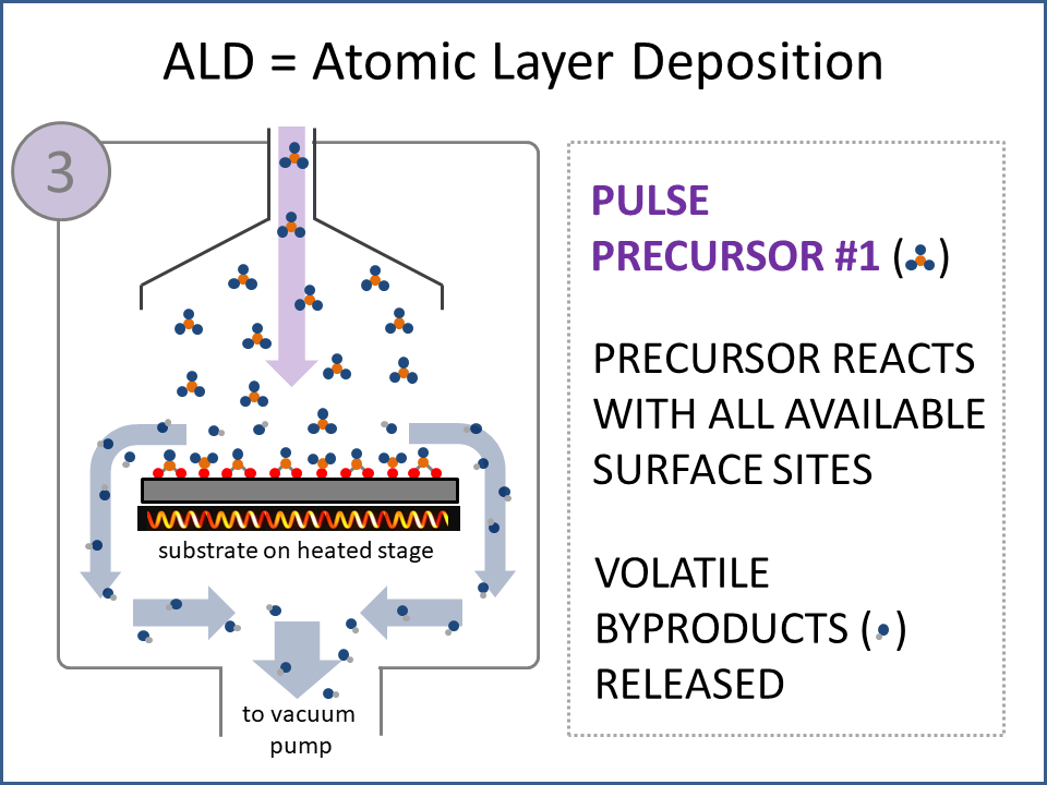
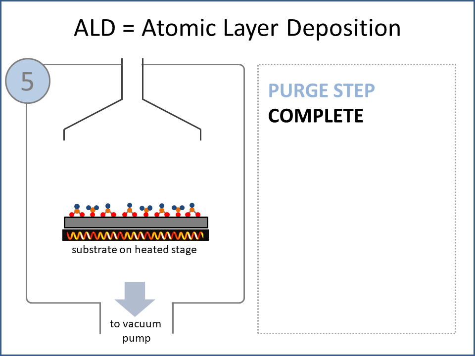
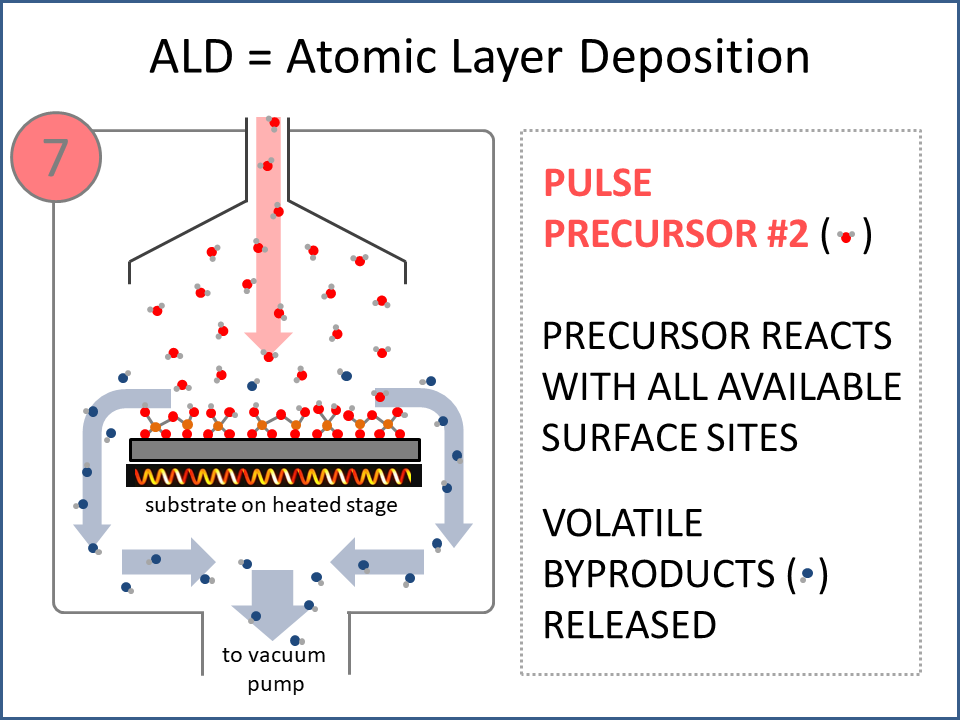
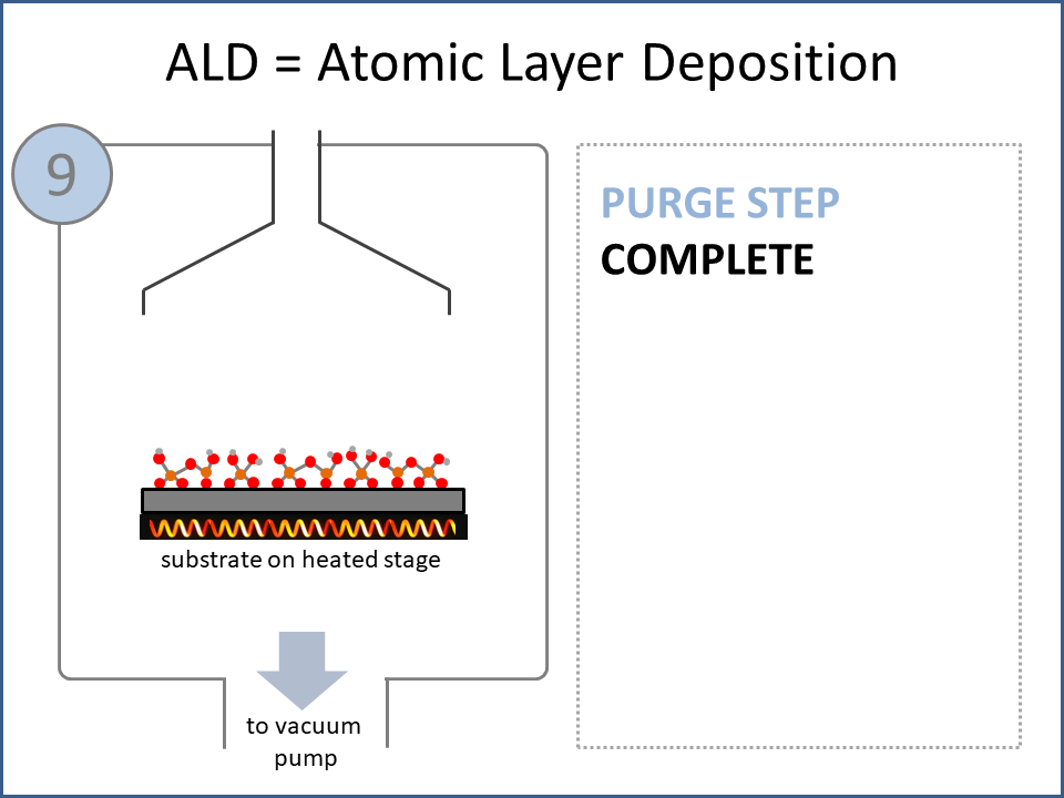
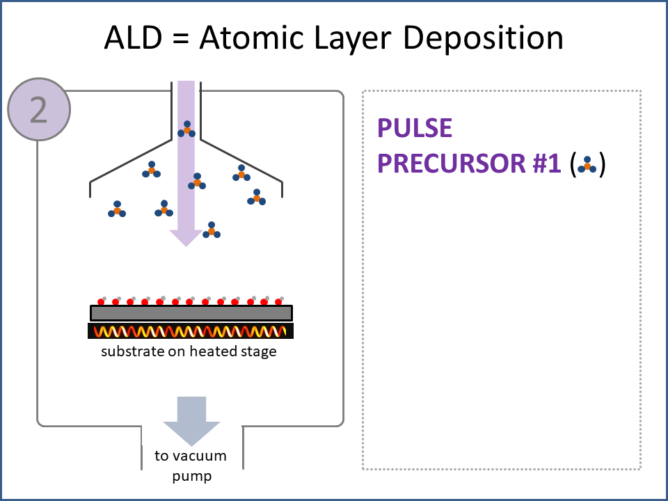
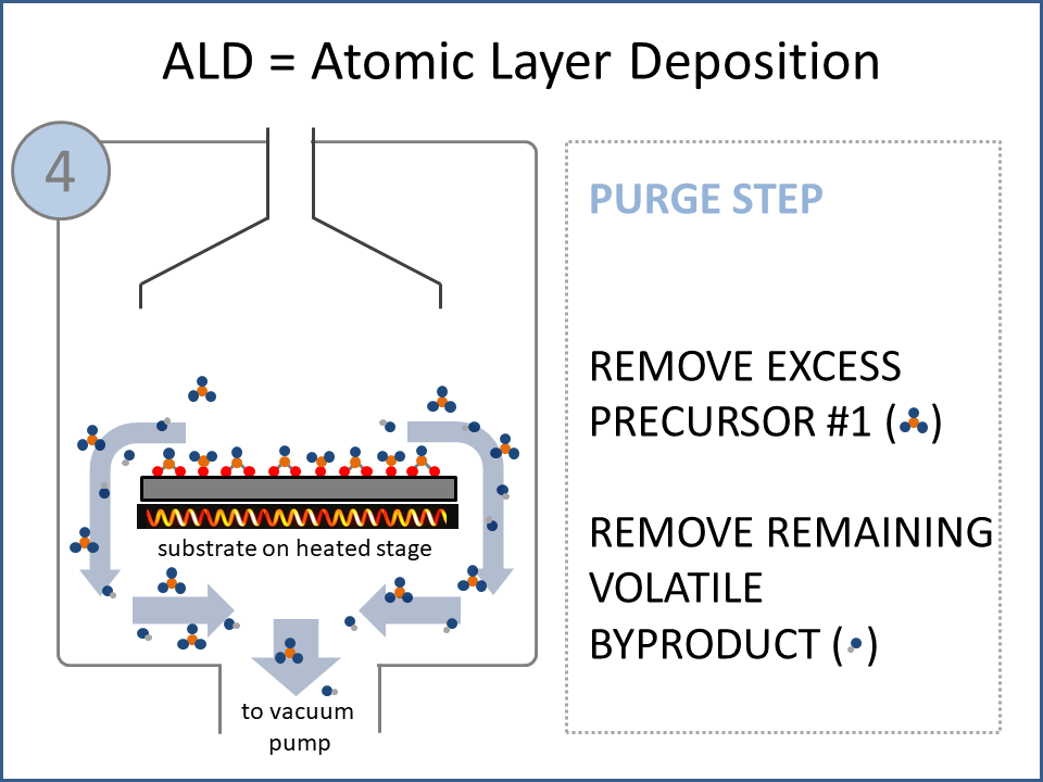
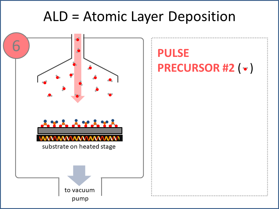
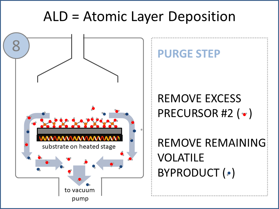
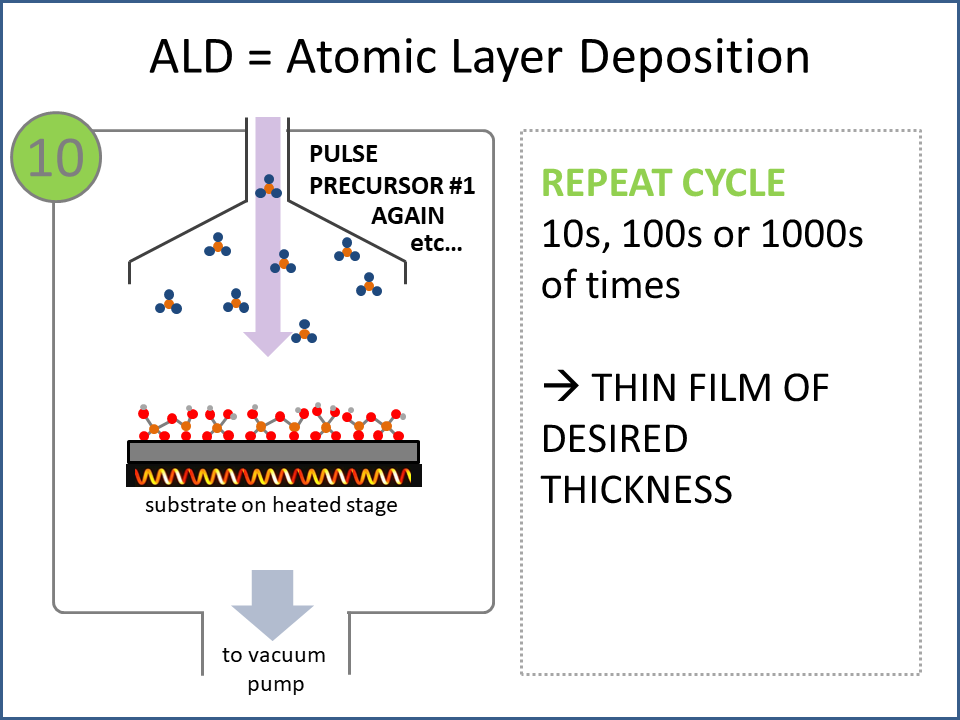
ALD Film Growth: Atomic Layer Deposition (ALD) is a thin film deposition technology that relies upon surface-based chemical reactions between 2 or more precursor molecules which are sequentially delivered to the substrate surface in the vapor phase, as shown in the sequence of images (1-10) on the right hand side.Film growth is achieved using 10s, 100s or 1000s of ALD cycles, each one typically consisting of a precursor pulse, followed by a purge step, a pulse of a different precursor, and then another purge step. The reactions involved in ALD are self-limiting, meaning that they proceed until all available surface sites have reacted, and then they stop. This means that a substrate can be exposed to sufficient precursor to ensure complete reaction at all available surface-sites, even at the bottom of deep trenches and under overhangs, and within each ALD cycle, exposure to more of the same precursor molecule does not result in thicker films. ALD Advantages: As a consequence of self-limiting reactivity, ALD is uniquely capable of depositing extremely uniform and conformal (i.e. surface-hugging) thin and ultrathin films (typically 2-500 nm) with high interface quality, even on high aspect-ratio substrates, and this can make the difference between a device which works, and a device which does not. Furthermore, ALD provides unparalleled control over film thickness, since this depends only on the number of ALD cycles (so long as the precursor pulses are above a minimum duration required to ensure complete surface reaction). In addition, since ALD does not rely upon (and in fact must avoid) thermal decomposition of the precursor molecules, ALD film growth can typically be achieved at lower temperatures than CVD (see below); often < 200°C, and sometimes even at room temperature. For these reasons, ALD is used in various industrial applications (e.g. deposition of HfO2 in computer chips, Al2O3 in Dynamic Random Access Memory, and ZnS in electroluminescent displays), and the applications for ALD are rapidly growing. ALD challenges: A major challenge in ALD is that different precursor molecules and surface-based reactions are required for ALD of each different thin film material, and for many materials, suitable molecules and deposition reactions have yet to be conceived. Furthermore, many known ALD methods do not yield films with sufficient purity for a particular application, or require conditions which are thermally or chemically incompatible with the substrate upon which ALD is required. This is especially the case for ALD of many pure elements, which is particularly challenging; much more so than methods for ALD of oxide and nitride thin films, which are more established. Thermal vs Plasma ALD: ALD can be achieved with or without the use of plasma-generated reagents; referred to as thermal ALD and plasma-enhanced ALD (PEALD), respectively. For some materials, only PEALD methods have been realized. However, thermal ALD is generally preferable, since PEALD requires a more complex and expensive experimental setup, can result in substrate damage (due to plasma and/or UV exposure), and can experience problems conformally coating nanoscale high aspect ratio structures, since highly reactive plasma-generated species often re-combine before reaching the bottom of deep trenches (this is especially the case for plasma-generated hydrogen radicals on metal surfaces). Other techniques for thin film deposition (PVD and CVD): Other techniques for thin film deposition include PVD (Physical Vapor Deposition) and CVD (Chemical Vapor Deposition). PVD refers to a variety of vacuum deposition methods, including magnetron sputtering, thermal evaporation, and electron-beam evaporation (a simple schematic for metal thermal evaporation is shown below; the substrate is rotated, often with heating or cooling). CVD involves thermal decomposition of volatile molecules (delivered in the vapor phase) upon contact with the surface of a heated substrate (a schematic is shown below, with molecules entering the reaction chamber via a "shower head").
Both PVD and CVD are widely used in device fabrication. However, neither technique results in self-limiting growth. Therefore, both PVD and CVD experience problems depositing highly uniform and conformal ultra-thin films, especially on substrates patterned with high aspect ratio features such as deep trenches, overhangs, or vias, and these issues become increasingly significant as the thickness of the target films decreases.
|
|
|

